
Koala TetraProbe - Electrical characterization at the nanoscale
Ultra Compact Multi-Tip Scanning Probe Microscope / Nanoprober for electrical characterization at the nanoscale.
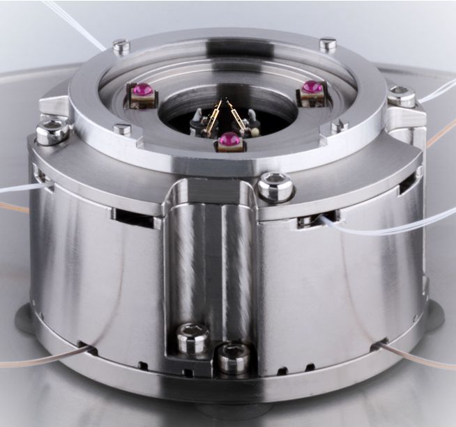
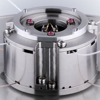
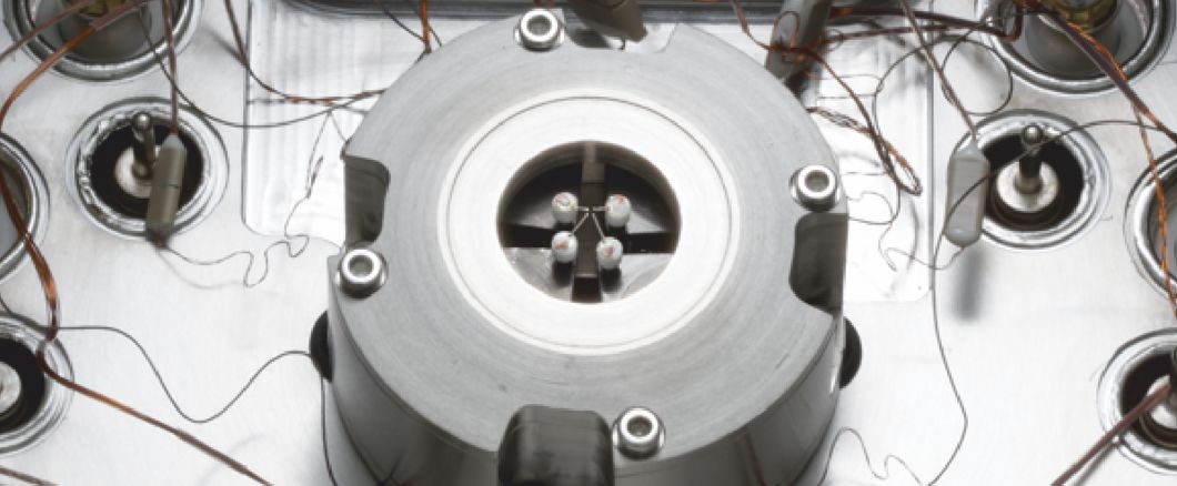
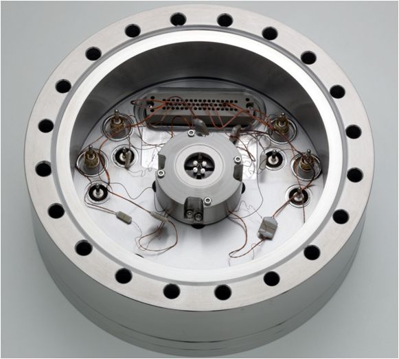
The ultra compact Koala TetraProbe STM integrates four independent STM units within a diameter of 50 mm resulting in an unsurpassed mechanical stability, enabling atomic resolution imaging with each tip.
Features:
-
Modular and compact design based on the KoalaDrive® nanopositioner
-
Each tip can be positioned independently
-
Tip coarse positioning with optical microscope/SEM control
-
Simultaneous tunneling and scanning with all four tips
-
Atomic resolution with each tip
-
Tip exchange and sample exchange in situ
-
Software controlled switching between current probe and voltage probe for each tip
-
Software allows virtually any possible "concerted" spectroscopic measurements involving the four tips and the sample
-
Four tip STM/AFM combination and low temperature version available
Applications:
-
Local potential measurements on the nanoscale
-
Controlled nondestructive measurements in spectroscopy mode
-
Four point measurements with free positionable local probes on structured samples
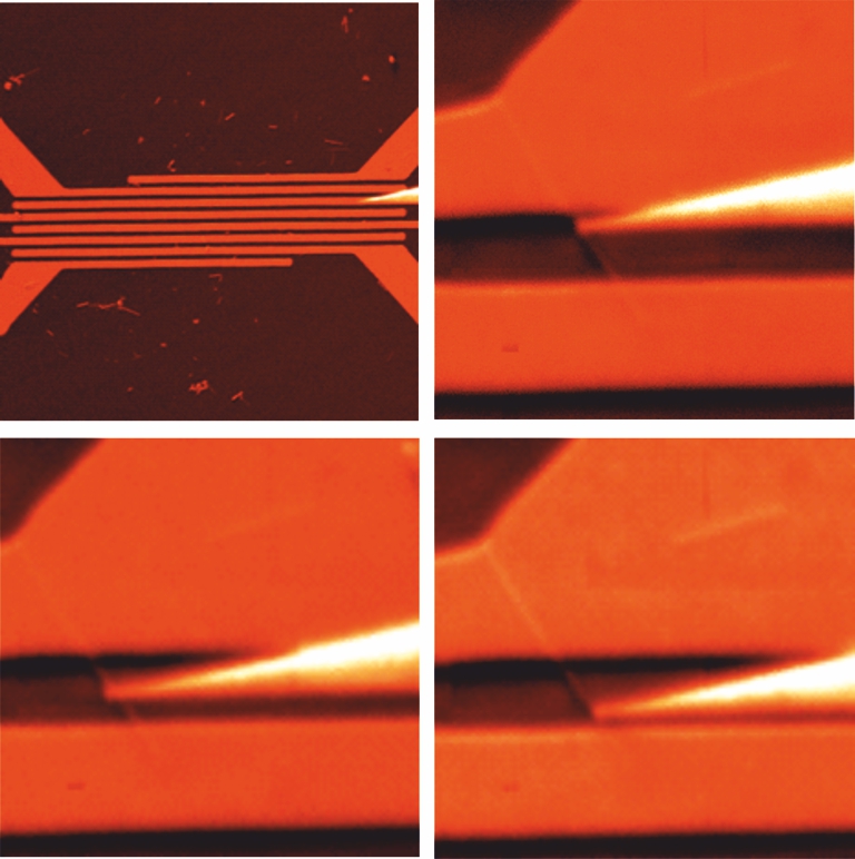
Real time optical microscope movie of the positioning of the sample and four tips on a structured wafer. The structured rectangles have a size of 30 μm x 50 μm.
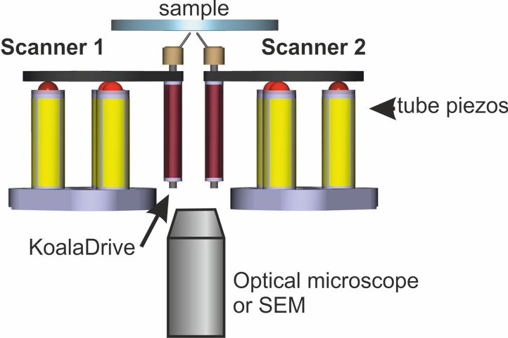
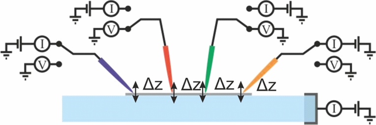
Sketch of two of the four modular units of the Koala TetraProbe. Each unit consists of a KoalaDrive used for the coarse tip approach towards the sample. The KoalaDrive is fixed to a plate (resting on three balls fixed to three tube piezo elements). The plate is moved according to the design of the beetle STM allowing for a coarse motion in the xy-directions. The xyz-scanning of the tip is also performed by these three piezo elements.
 |
 |
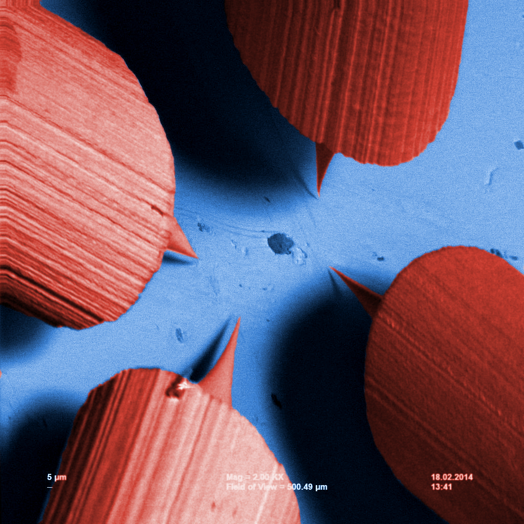
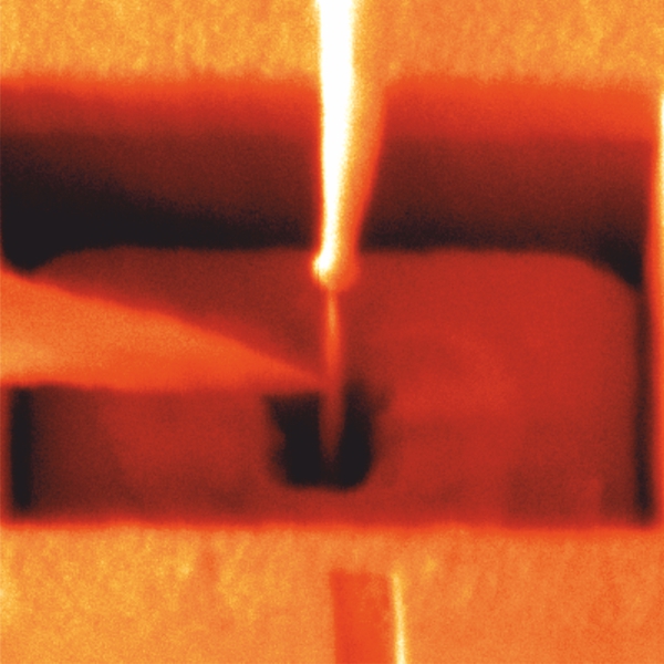
SEM view of the tips. Tip shadows indicate the tip-sample distance
Results:
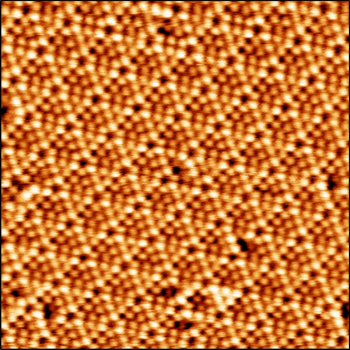
Atomically resolved image of the Si(111)-7x7 surface |
 |
Surface conductivity determined by distance dependent four probe measurements:
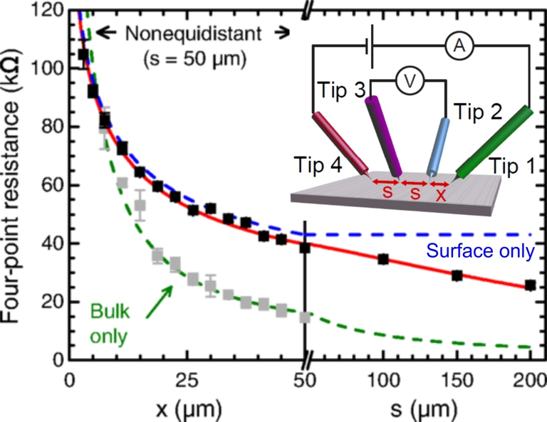 |
The surface and step conductivities of the Si(111)-7x7 were measured. More information can be found in Phys. Rev. Lett. 115 (2015) 066801. |
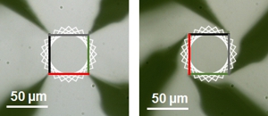 |
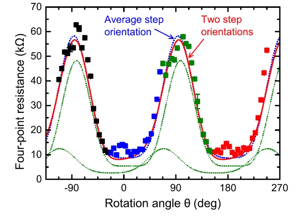
The anisotropy of the surface conductance can be determined using rotated tip configurations (optical microscope view). More information can be found in Phys. Rev. Lett. 115 (2015) 066801. |
 |
|
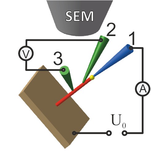
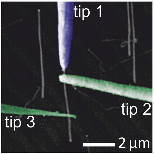
Resistance / dopant profiling along freestanding GaAs nanowires:
|
 |
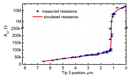 |
Resistance profile along a nanowire. More information can be found in Appl. Phys. Lett. 103 , 143104 (2013). |
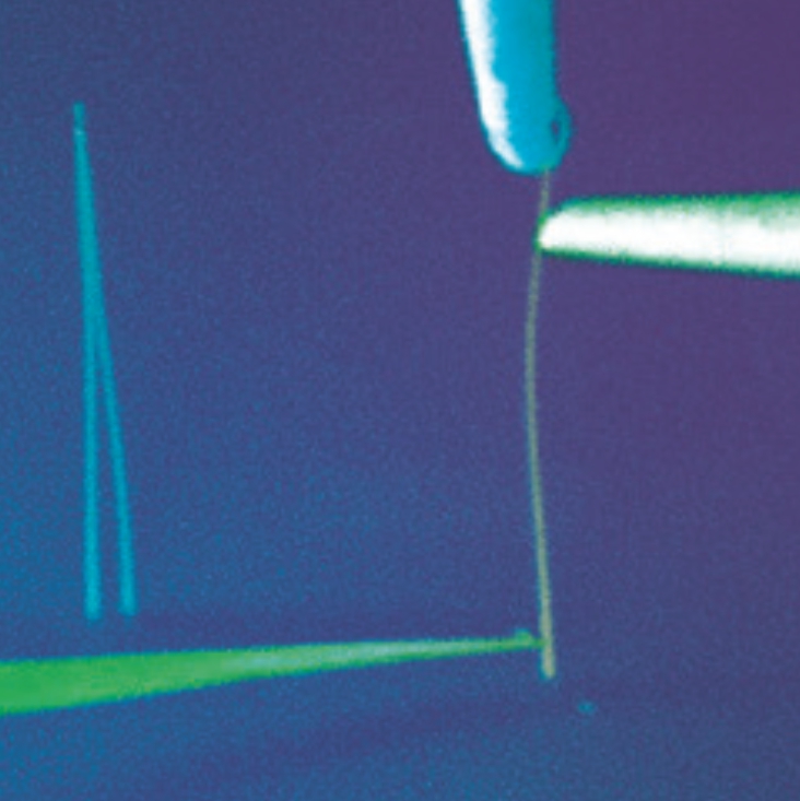 |
Movie of an STM tip moving along a GaAs nanowire measuring a four point probe resistance profile
Movie of an elastic bending of a GaAs nanowire (left). SEM zoom to nanowires (right).
Scanning tunneling potentiometry with a four tip STM:
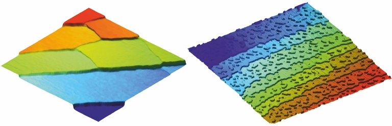
(left:) Potential map on a Si(111)-7x7 surface during current flow from top to bottom. (right:) Potential map of a Si(111)/Ag-sqrt3 with overlaid topography. More information can be found in here.
Multiprobe measurements on Sb2Te3 nanowires.
Potential measurements along a 2 μm long wire segment.
Multiprobe measurement on a freestanding topological insulator nanowire:
Customer specific extensions, like for example optical fibers brought close to the tip/sample regions by a fiber positioner integrated in the TetraProbe system can be provided. A low temperature version of the TetraProbe system is available as well.
Some results are discussed this application note
The KoalaDrive® is licensed by Forschungszentrum Jülich
We offer SPM solutions according to your specific requirements.
Please do not hesitate to discuss your requests with us.
Any inquiry can be sent to: info@mprobes.com